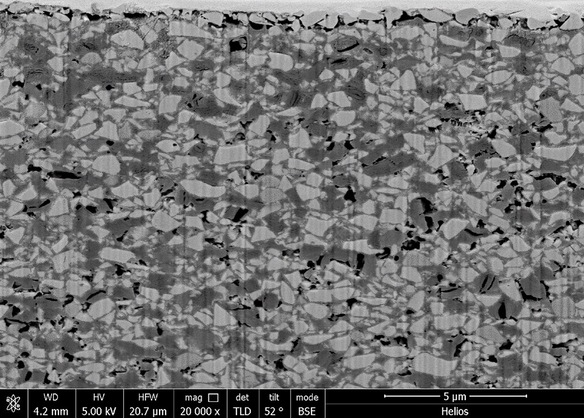
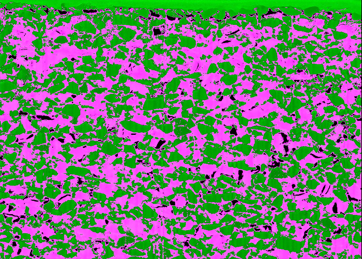
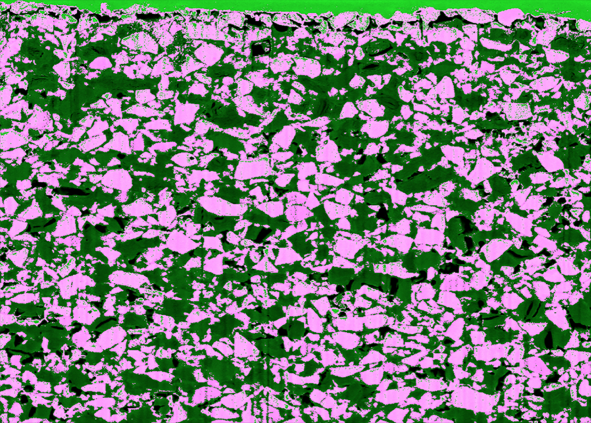
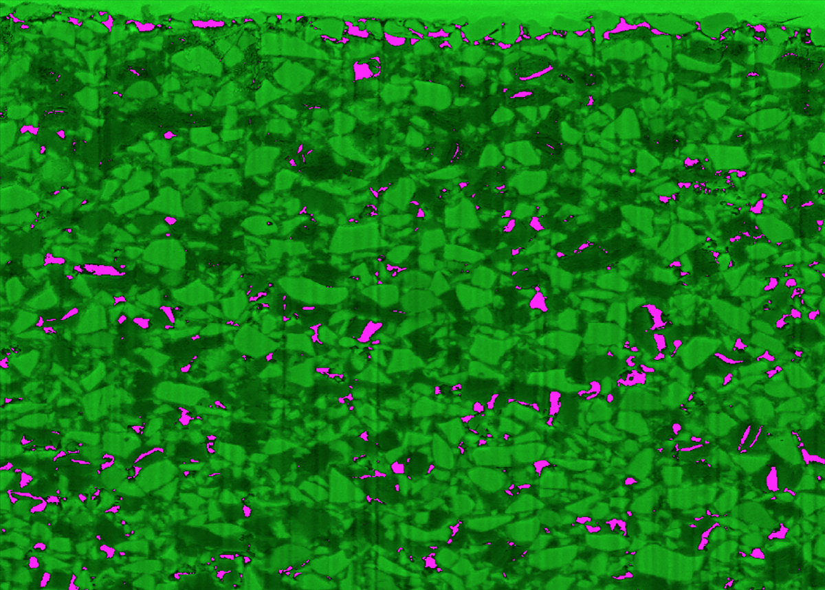
Analysis Of Third Party Images
ApplicationsIntegrate Your Analysis from Multiple Tool Types
Wafer inspection is becoming more challenging and costly at each node. The production process lead time for bringing integrated circuits to market is rising. Complex inspection, testing, and validation procedures can create delays.
Having one tool that can analyze images from all your other tools can save time and increase throughput.
Whether the images are from an e-beam or an optical inspection system, Nanotronics software can analyze the images at every process step and prepare customized reports for tracking manufacturing, assigning defect causality, and giving corrective feedback.
The software has several analyzer types and the settings are fully customizable. There are also four defect report viewing modes. Nanotronics software can connect all the inspection devices in your fab so you can find correlations between defect-identification data and process-tool parameters and make timely corrections to fabrication tools.