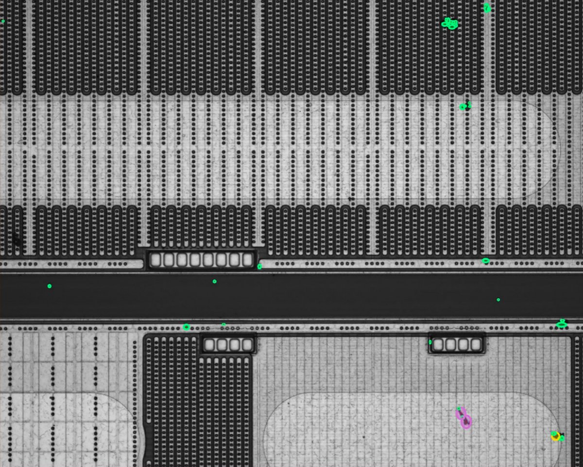
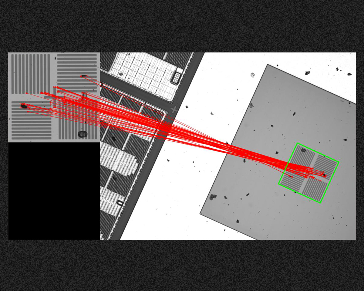
Device inspection uses a Golden Die without defects that meets your performance design and then compares that die across your patterned wafers. Our device inspection process will
detect defects caused by particles as well as systemic defect clusters caused by the photomask or the exposure process.
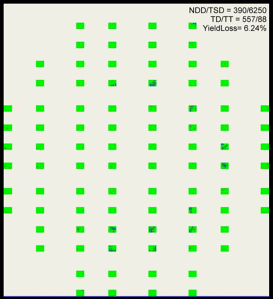
The inspection process generates a defect map that reports all defects detected and the process works for very large devices and detects defects on regions of undifferentiated high-frequency features.
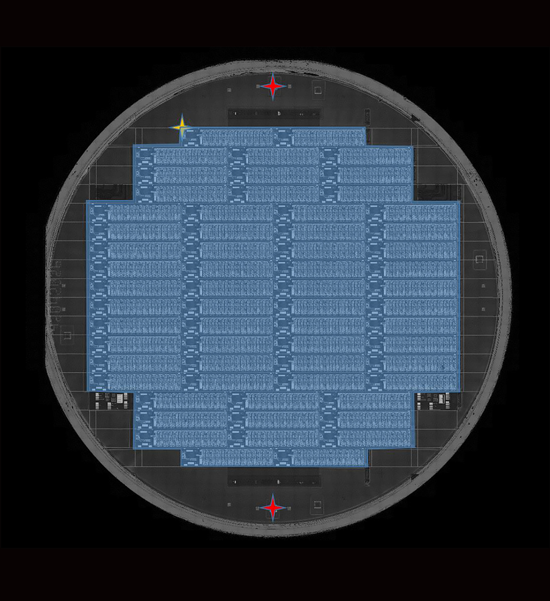
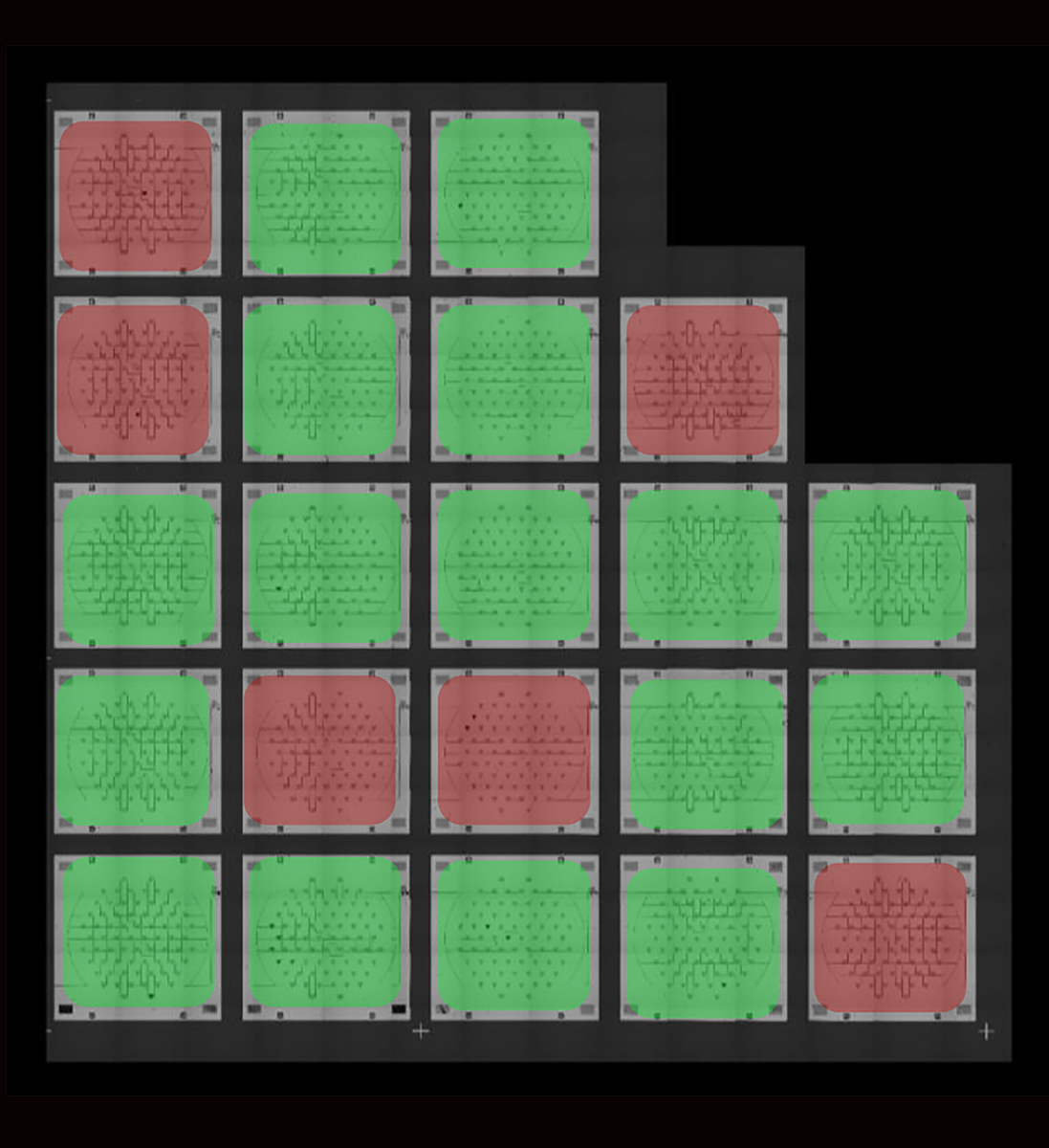
Device inspection can be done while the devices are on the wafer or in gel packs or laid out on tape. An annotated virtual mosaic is then created with summary statistics that include overall yield and Pass/Fail results and the results are exportable as .csv and can be integrated with KLARF and SECS/GEM.