nSpec® LS
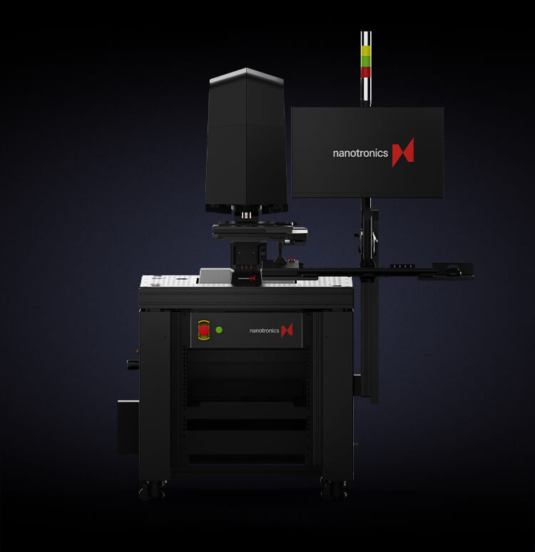
nSpec® LS
Combining optical microscopy, computational super resolution, artificial intelligence, and robotics, Nanotronics is bringing the world’s most advanced wafer inspection microscope to every manufacturing sector.
Learn MoreThe World's Most Advanced Inspection Tool
The inspection system design allows for easy set up of repeated quality control testing, in addition to settings for single image capture or scans. Configuration options include wafer size, types of defects to be identified, and scan resolution. An optional wafer loader and various sample chucks are available to meet specific needs. Nanotronics offers nTelligence™, a suite of consulting services as a part of nSpec®, for training, building, and deploying AI pipelines. Contact Nanotronics to see how nTelligence™ can improve your research, development, and manufacturing environments.
nSpec® LS
Optical Inspection For:
- Substrate Wafers
- Epi Wafers
- Patterned Wafers
- Diced Wafers
- Individual Devices
Features
nSpec® LS
Specifications
-
Travel, typical
200 mm X and Y direction
-
Centered Load Capability
2.27 kg
-
Repeatability
+/- 0.5 μm
-
Step Size
0.04 μm
-
Travel Flatness
30 μm
-
Weight
54 kg
-
Limit Switches
Mechanical, non-adjustable
-
Wafer Vacuum Chuck (optional)
Adjustable to 50, 75, 100, 150, 200, or 300 mm
-
White Illumination:
LED (other options available)
-
Brightfield/Darkfield Objectives:
5, 10, 20, or 50x, user selectable
-
Differential Interference Contrast:
(Normarski)
-
Stage, Focus, Nosepiece, Illumination, Camera
Manual user operated