January 8, 2024
Blog
What is Wafer-Level Packaging, and What Forms Does it Take?
Modern industry is largely driven by the ability to scale at a rapid pace, which requires harnessing the most cutting-edge technology to boost efficiency at every turn. Continuous innovations in semiconductor development are vital to expansion and profitability, and wafer-level packaging is elemental in that method.
This article will address the importance of wafer-level packaging, the different forms the process assumes, and strategies adopted by manufacturers to meet the quality-control challenges that accompany transformative semiconductor technology.
What is Wafer-Level Packaging?
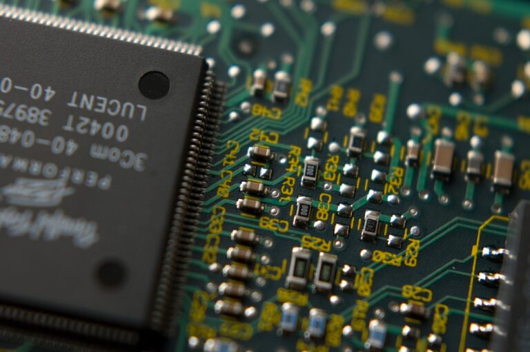
Wafer-level packaging (WLP) is an advanced process that has risen from the continuous demand for more powerful CPU’s and the need to increase production capacity for devices such as mobile phones and smart devices connected to the Internet of Things (IoT).
WLP is a precise, intensive process that involves attaching components to integrated circuits (ICs) before a wafer is diced. This is unique from other processes in which the wafer is diced into circuits before packaging components. Before WLP, wafers had to be sliced into individual circuits before they were packaged.
Chip-Scale Packaging (CSP)
Wafer-level packaging is a form of chip-scale packaging (CSP), a technique used to miniaturize ICs. CSP originally stood for “chip-size packaging”, but over the years, manufacturers have continued to shrink the size of semiconductors, shifting the definition of CSP in reference to chip scale. Wafer-level chip-scale packaging (WL-CSP) creates the smallest package currently in production, a tremendous achievement within the contemporary technological landscape.
What Are the Benefits of Wafer-Level Packaging?
Wafer-level packaging significantly decreases chip size, wiring length, and other elements of PCB circuitry. This makes it possible to integrate packaging, testing, and burn-in, which minimizes costs, increases production, reduces power consumption, and improves overall device performance.
WLPs make designing increasingly sophisticated and powerful devices like smartphones and laptops possible while continuously driving manufacturers to scale performance, quality, capacity, and cost savings.
As a result, manufacturers can produce semiconductors with smaller, thinner, and lighter packages that meet the high-performance demands of the telecommunications, healthcare, computing, and transportation industries, amongst others.
Types of Wafer-Level Packaging
WLP takes the following primary forms:
Wafer-Level Chip-Scale Packaging (WLCSP)
WLCSP produces the smallest form of WLP, in which the package size is almost identical in size to the die. Solder balls are formed directly over the wafer without an added substrate.
WLP integrates fabrication and testing at the wafer level for more efficient manufacturing, reducing costs and increasing capacity without sacrificing quality. Because WLP is a form of chip-scale packaging (CSP), associated processes are often referred to as WLCSP as well.
A WLCSP is a bare die with a redistribution layer (RDL) for managing connections, inputs and outputs (I/Os), and virtually unlimited circuitry designs.
Fan-In WLP (FI-WLP) and Fan-Out WLP (FO-WLP)
There are two main forms of wafer-level packaging: Fan-In WLP (FI-WLP) and Fan-Out WLP (FO-WLP). Both fan-in and fan-out wafer-level packages use an interposer, which provides the electrical connection between the die and components in a package.
In both FI-WLP and FO-WLP, the interposer is the connection between semiconductor die and package substrates. With FO-WLP, the interposer is larger than the die, and with FI-WLP, it is the same size.
Fan-In Wafer-Level Package (FI-WLP)
FI-WLP involves packaging ICs at the wafer level. It is a method of chip-scale packaging (CSP), given that the final package and die are the same size. A redistribution layer (RDL) connects the I/Os to solder bumps on the die surface.
Fan-Out Wafer-Level Package (FO-WLP)
The FO-WLP involves dicing silicon wafer chips on a carrier panel with a redistribution layer on top of the die and the mold. The chip is placed on a larger wafer where an RDL connects the chip’s I/O points to the carrier’s surface, causing the I/O points to “fan out” past the chip’s dimensions. This allows for improved electrical performance while reducing the package size.
RDL-Fist Process
RDL-Fist is a FO-WLP process where the RDL fabrication precedes chip placement.
What is the Difference Between FI-WLP and FO-WLP?
While both packaging processes dramatically improve manufacturing scale and efficiency, there are several distinctions between FI-WLP and FO-WLP.
-
1. Device Size
With FI-WLP, the packaged device is the same size as the die, while the FO-WLP packaged device is larger than the die.
-
2. Number of Pins
On FI-WLP devices, all pins are located on the bottom of the chip, which limits the number of pins. On a FO-WLP device, it is possible to have a larger number of pins because they may exceed the chip’s size by design.
-
3. Complexity of Design
The FO-WLP process enables more complex and detailed designs as is has the unique capacity to include more pins.
-
4. Device Production Cost
FI-WLP production are often more economical, requiring fewer I/O connections and far less materials.
Wafer-Level Packaging Process Flow for FO-WLP
The FO-WLP process assumes two different forms: Face-Up FO-WLP and Face-Down FO-WLP.
Face-Up FO-WLP Process
- 1. The semiconductor is placed face-up on a wafer.
- 2. The chip and its carrier are molded together to provide mechanical support and protect the chip.
- 3. RDL fabrication is applied to intiate the fanning out of I/O points.
- 4. Solder balls are attached to connect the packaged chip to the parent circuit board.
- 5. The packaged chip is removed from its temporary carrier through debonding.
Face-Down FO-WLP Process
Face-Down FO-WLP is performed the same as Face-Up, but with the semiconductor facing down.
Wafer-Level Packaging Process Flow for FI-WLP
The FI-WLP Process involves the following steps:
- 1. RDL fabrication through a process such as photolithography or electroplating
- 2. Attaching solder balls to form electrical connections
- 3. Thinning the wafer
- 4. Cutting the wafer
- 5. Testing the final package
How to Reduce Quality Issues with Wafer-Level Packaging
The benefits of using WLP are extensive. Manufacturing will continue to trend towards perfecting wafer-level packaging processes to increase resulting innovations.
However, the same qualities that lead to greater efficiency and reduced costs—their size and intricate design—will push manufacturers to address new precision challenges in identifying defects, both in original source materials and final products.
Semiconductors may take several months to complete, which means manufacturers must take measures to adjust operations at a level of intricacy that meets the advanced requirements of the complex circuits they produce.
The Power of AI-and-ML-Based WLP Handling and Scanning
Quality control for miniaturized circuits is complex but vital for preventing costly downtime. That’s where Nanotronics’ expertise lies: assisting manufacturers with advanced imaging, detection, classification, and assigning causality to nanoscopic flaws.
Nanotronics builds AI and machine learning hardware and software for comprehensive inspection throughout the lithography/patterned wafer manufacturing process, allowing you to:
- 1. Detect subtle defects
- 2. Limit false positives
- 3. Reduce expenses
- 4. Report defect data to eliminate defective dies from later manufacturing stages
Enhance the efficiency of your operations with more up-time and data-driven cost-savings by contacting the Nanotronics team today.